Erik R. Hosler, FylEx
Introduction
The economy of scale is essential for both science and industry. Quarks, gluons, and the Higgs boson (to name a few) would all have gone undiscovered without the economy of scientific scale, where particle accelerators are essential to access the energies at which these fundamental particles can be observed. The accelerator community has pushed the frontier of scientific discovery for decades with innovation to build more powerful and capable machines. From particle “smashing” accelerators to accelerator-driven free-electron lasers[1-3], each machine generation has necessarily improved the cost, footprint, and manageable beam current per GeV of acceleration, driving the economy of scale and further proliferating accelerator applications and avenues of scientific investigation [4-6].
Similarly, our modern society would not exist without semiconductor “gigafactories” [7]. Moore’s Law is predicated on the idea that creating more transistors per square area will lower the intrinsic, per unit manufacturing costs, and while the cost of building a semiconductor factory doubles every four years (Rock’s Law) [8], rising to north of $20B today [9]. Nevertheless, Moore’s Law is most certainly alive, and thriving, in the age of Artificial Intelligence (AI) [10-12]. However, just like data center scaling in support of inference engines [13-15], the environmental toll of ultrascale integration (even in conjunction with advanced packaging strategies) semiconductor manufacturing has become staggering [16]. Taiwan Semiconductor Manufacturing Company (TSMC) currently consumes more than 9% of Taiwain’s entire electrical capacity and will need an additional 2% in the coming years, amounting to 60% of the planned national capacity [17]. This equates to three nuclear reactors worth of electricity [18-20]. At the center of this massive electrical consumption is a singular manufacturing tool, the extreme-ultraviolet (EUV) photolithography scanner.
Light is a critical enabler for leading-edge semiconductor manufacturing. The properties, quality, and quantity of lithographic light determine the manufacturable device performance and economics, and have been the backbone of Moore’s law economics [21-24]. By extension, innovations in light source technology have enabled tectonic shifts and consolidation in the semiconductor industry, where the use of EUV lithography is a dividing chasm between advanced and legacy technologies. For example, sub-7nm nodes, which require EUV lithography to be economically viable, are 59% of TSMC’s earnings but <400k out of an installed ≃15M 300mm equivalent wafer start capacity [25, 26]. With both the highest investment and profitability skewed toward leading-edge technologies, and the subsequent consolidation of skilled labor around those at the forefront of its development and execution, the competitive landscape disproportionately favors the leaders. These skewed economies of scale divide not only technologies but also the commercial marketplace and, by extension, national economies. Recent worldwide legislation has striven to break down the centralization of advanced semiconductor manufacturing in the face of these economic hurdles [27], however, this expansion of domestic capability-enabling capacity will only exacerbate the overall carbon footprint and environmental challenge of the industry [28]. While light is the enabler for advanced semiconductor manufacturing, it has also become an essential triad for technology leadership, security, and economics.
EUV scanners, built by ASML, are the most advanced lithography tools in the world. Utilizing 13.5nm light, generated by a tin laser-produced plasma (LPP), features as small as a few nanometers can be printed with angstrom precision [29, 30]. Advances in sources, optics and mechatronics allow each new lithography tool generation to print smaller features at higher precision (overlay and edge-placement error reduction) [31] thereby establishing the transistor technology ground rules, i.e. what is the most advanced chip a fabless (e.g., Nvidia, AMD, Microsoft, Mediatek, Qualcomm, etc...) or integrated electronic device manufacture (e.g., Intel, Samsung) can manufacture [32]. Here, there is a distinct difference between a demonstrable process technology and a manufacturable one. While there are certainly many novel proposals and demonstrations of both unique device architectures pushing the boundaries of electronics [33, 34], the ability to produce trillions of devices per 300mm wafer with yields targeting 90% or better requires substantial process engineering and an in-depth knowledge and control of semiconductor capital equipment [35, 36].
EUV lithography has several distinct differences compared to prior lithography technologies, specifically when it comes to the photochemical mechanisms and the interplay between light source power scaling and optical column transmission impact the cost efficiency of the patterning process [37-40]. As target feature size and desirable pattern roughness decreases, the necessary photoresist dose (i.e., the energy required to resolve the target feature) increases, which implies that the number of incident EUV photons per unit area must proportionately increase to maintain the EUV scanner productivity (i.e., processed wafers per hour). EUV’s financial viability is therefore strongly tied to source power, which has drawn the industry to constantly be looking for ways to increase the deliverable photon flux on wafer [41].
Evolution of Accelerators and EUV Lithography
Free-electron lasers and EUV lithography both have their origins in the 80’s and 90’s [42-46]. In the subsequent decades of mutual maturation, an interwoven history of advocation and speculation has existed concerning whether the two technologies would become mutually supportive and enabling. Shortly after the creation of the EUV-LLC [47, 48], when the choice of EUV light source was far from clear, FELs were proposed as a potential light source capable of generating kWs of extreme-ultraviolet light in support of lithography [49, 50]. There have been multiple design iterations as accelerator and FEL technology advanced, but regardless of configuration, the requirement of multiplexing a single light source to multiple end-stations (lithography tools) persisted as a result of cost and scale [51-55]. While compact versions were proposed, insufficient progress was made toward viability, and moreover, the designs were insufficiently compact [56-60]. Fab’s require that each tool in the cleanroom maintain its support equipment in the subfab within the same footprint as occupied in the ballroom. This allows for optimal tool compaction and modularity in layout. While EUV lithography has become a necessary exception, space remains at a premium both in and around a cleanroom [61], and given the risk averse attitude to paradigm shifts in the semiconductor industry [62, 63], adoption of the ”multi-user” light source facility (e.g., synchrotron or FEL) was viewed as a non-starter.
A critical inflection point occurred in 2013 with prognostication of the 7nm technology node heralding the demise of Moore’s Law. The patterning requirements at 7nm necessitated either costly 193 nm immersion lithography multipatterning or EUV lithography, which was delayed primarily because of the EUV light source [64-66]. As semiconductor manufacturers expressed concerns over the source power roadmap [50], concerted analysis began within the industry to evaluate the state-of-the-art of accelerator and FEL technology as a viable lithography light source [67]. Multiple study programs were launched, most notably by ASML [68], a consortium of US National Labs and RadiaBeam, KEK [69], and GLOBALFOUNDRIES [70]. Although there were variations in the final design recommendations between the various programs, common threads emerged. The economy of scale for an accelerated-based lithography sector would indeed necessitate simultaneous multiplexing across multiple end-stations (lithography tools). Specifically, efficient creation and distribution of multiple, independent photon beams would be essential. Moreover, the ability of the light source to provide light to each end-station at near 100% availability was critical but highly suspect. For context, a semiconductor fab producing 100k 3nm wafers a month generates up to $3M per hour in revenue.
Several solutions emerged to resolve both the distribution and availability concerns. For an electron accelerator driving a free-electron laser, either the electron or the photon beam could be divided to service multiple end-stations and were publicly proposed by GLOBALFOUNDRIES [71-73]. Electron multiplexing had long been enabled at the Jefferson Accelerator Facility CEBAF machine [74], and photon beam splitting at free-electron lasers had recently been demonstrated at FLASH and LCLS [75-78]. To resolve concerns regarding availability, redundancy was proposed to first order, where two accelerators housed in separate radiation vaults would allow safe maintenance in operation of the overall complex [79, 70]. Furthermore, the exact configuration of the accelerator in conjunction with the maturity of the constituent hardware was highlighted as essential for industrial operations [73].
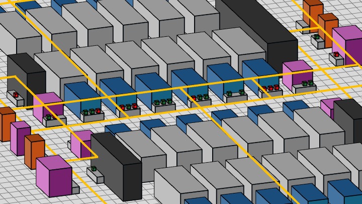 Figure 1: Illustrative layout of a lithography sector in the semiconductor fab cleanroom. Gray is lithography scanner, blue is process track, orange and pink are various metrology and inspection tools, black are mask and wafer storage, gold is overhead transport of wafers in either red or green pods.
Lastly, while it is common place for particle accelerators to be the center point of scientific user facilities, the equipment paradigm in semiconductor manufacturing focuses on independent, self-contained, unit scalable hardware. Industrial engineering relies on this modularity for scale and operational efficiency (e.g., flexible routing between matched tools, avoiding single-point congestion, product staging, etc...). Moreover, the economy of scale relies on phased capacity construction. This allows for technology process research and development to be conducted on the exact (or very similar) tools as will be used for volume production simply by increasing the number of tool copies. Prior to 2019, it was an annually revisited open question within the semiconductor industry as to whether EUV lithography was ready for high-volume manufacturing (HVM), or if it ever would be, tracked by a scorecard at the International Symposium on EUV Lithography. In light of this existential question, in conjunction with the industrial engineering requirement of “copy exact” between R&D and HVM equipment, the idea of building a large scale light source facility to solve one of several outstanding critical issues faced by the industry (defectivity impacting device yield was another challenge) [80, 81] was deemed too high risk.
In 2019, TSMC announced the introduction of EUV process into HVM through their N7+ technology node [82], and ever since it has been a race within the industry to install the most EUV lithography scanners and operate them most efficiently/effectively to drive time-to-market and product yield. It was no longer a question of ‘if’ EUV lithography would be used but how much could the technology be leveraged to drive transistor density and performance, opening a new avenue for the economy of scale within Moore’s Law. Now, in 2024, EUV sustainability is challenged [83] by the megawatts of electrical power, hundreds of liters of hydrogen per minute, and thousands of gallons of water required for each high-end lithography scanner [84, 18]. Irrespective of the sustainability challenges, the industry must also expand EUV lithography capability by increasing the numerical aperture [85, 83], improving depth of focus [86], minimize stochastic effects [87], increasing source power [29], improve overlay performance, minimize k1 [88], and ensure toolset flexibility [89].
FEL Industrialization and Photolithography
The semiconductor industry will strive to resolve the future lithography challenges utilizing the proven LPP architecture, however, there is renewed interest in developing FEL sources for lithography now that EUV is entrenched as the driving force of leading-edge manufacturing. Evaluating the future EUV lithography challenges reveals advantages for a utility scale FEL light source, and has sparked the formation of several start-up companies and activity from established contributors.[90, 16, 91, 53, 54] Moreover, state-of-the-art innovations in high-repetition rate, superconducting accelerator-based FELs (e.g., LCLS-II [92, 93] and XFEL [94]) highlight the maturity of critical components and infrastructure necessary for an industrial-class accelerator facility [95]. Recent discussions within the FEL community have further highlighted the lack of technology showstoppers as well as strong confidence in the established component hardware (cryomodules, accelerator cavities, cryogenic plants, undulator magnets, conventional steering magnets, ultrafast lasers, solid-state RF amplifiers, etc...) [19].
Critical to the success of an industrial FEL program is a parameter optimization prioritizing robust operations. Focusing on system and sub-system uptime as well as stability of a limited number of desired output parameters is far less complex than most accelerator projects to-date. Unlike a scientific user facility, where capability and flexibility are required by design, an industrial light source can be engineered, even over-engineered, for a few applications or even a singular use case [96]. When compared to previously constructed accelerator facilities, an EUV FEL for lithography is more akin to the IR Demo than LCLS-(I/II/HE) [97, 92, 93]. As single purpose program originally, the IR Demo was designed to efficiently and decisively ’illuminate’ adversarial targets - to invent and prevent surprise [98-102]. With its fixed initial objective, the IR Demo was designed, green field built, and achieved its first power on target within three years, comparable to required industrial timelines. Comparatively, 10-20 years are typically required to plan and build a scientific user facility (e.g., LCLS was 11-years from design study[103] to ”first light”[104] and reused substantial existing infrastructure). Moreover, the IR-Demo is the only FEL to demonstrate 10’s of kilowatt-class performance and single operator start-up and operation, both of which are in-line with industry expectations.
Combining the engineering and operation modalities of the IR Demo with the maturation of accelerator components and technologies driven by FELs and accelerators over the past 25-years, an industrial FEL for the semiconductor industry can now be built with the necessary performance specifications [71]. In so doing, an accelerator-based industrial light source will become utility-scale infrastructure similar to water, gas, heat/exhaust, and electricity. Such a paradigm shift will reshape how light is both utilized and deployed in the fab, a shift which must be justified by the benefits. Projections indicate a reduction in EUV exposure cost approaching an order of magnitude with a similar reduction in the overall carbon footprint [16]. However, similar to other industrialized accelerator applications [105-108], FELs will need rigorous, fixed-purpose design, a robust supply chain of critical components, a trained workforce, and most importantly, a financially viable market. With the semiconductor industry as the market driver, and lithography as the targeted application, the critical components and workforce skills can be derived [70, 73]. Most critical will be the FEL cost and availability, as these will directly impact the heart of semiconductor economics. Beyond the semiconductor industry, there are numerous other potential drivers for industrialization, however, none of which has a comparable combination of need/benefit (both to the industry and society) and profitability.
FEL industrialization for semiconductor manufacturing will be a renaissance for the scientific community. With scale, comes dramatic reductions in costs throughout the supply ecosystem for accelerator components as a result of guaranteed demand. Should FELs be adopted for lithography applications, construction of five or more GeV-class accelerators will be built, per year. Establishment of a robust market will allow component suppliers and support infrastructure companies to reliably and permanently scale their facilities and capabilities. Moreover, the insatiable desire of the semiconductor industry for innovation (i.e., Moore’s Law) will continuously feed R&D in accelerator and FEL physics/engineering, similarly as it has many other fields (e.g., Semiconductor Research Corporation). This feedback between industry and the scientific community will lower the cost of major scientific user facility construction/operation as well as encourage student enrollment and study in STEM fields, fueling future scientific endeavors.
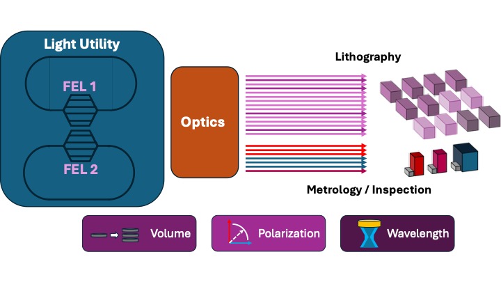 Figure 2: Diagram of an industrialized FEL light source utility for a semiconductor fab, incorporating redundancy and multi-application support leveraging the advantages in power scalability, light parameter selection, and wavelength tunability. All numerical aperture variations of EUV lithography can be driven at 13.5nm or shorter wavelengths while simultaneously powering metrology and inspection applications from 70-2nm.
Light source innovations have propelled Moore’s Law throughout the decades, with technology advances in lithography filtering through to other light-based fab operations (e.g., metrology and inspection). Introduction of a utility scale, accelerator light source promises to be the last light source innovation the industry will require given its intrinsic extensibility. Fab operations with an onsite FEL ensure availability of any wavelength or light parameter required with minimal carbon footprint and maximum reuse of technology. Furthermore, the expansion of metrology and inspection applications beyond capabilities of existing bulb, laser, or plasma light source provide an opportunity to expedite cycles of learning for both R&D as well as volume production/yield ramp. However, it is only with both the economy of scale of the semiconductor fab and industry as well as the scientific economy of scale within the accelerator and FEL communities that both can be overwhelmingly productive. Where historically light source technology has been an innovation stumbling block for the industry, accelerators will usher in an era of light-enabled innovation, expanding the transistor design space, and ensuring the longevity of Moore’s Law for the next twenty-five years.
Acknowledgments
I am indebted to Professor William Barletta, Harry Levinson, Moshe Preil, and Obert Wood for their insight and support to pursue accelerator physics for semiconductor applications. In addition, I am grateful to all those I have collaborated with throughout the last decade on FEL-based light source design considerations across the technical and leadership staffs at the US National Labs, worldwide accelerator facilities, and component manufacturers.
References
[1] F. Sannibale, “Particle Accelerators, A Historical Overview,” in US Particle Accelerator School.
[2] W. A. Barletta, J. Bisognano, J. N. Corlett, et al., “Free electron lasers: Present status and future challenges,” Nuclear Instruments and Methods in Physics Research, Section A: Accelerators, Spectrometers, Detectors and Associated Equipment 618(1-3) (2010).
[3] U. Amaldi, Particle accelerators: From big bang physics to Hadron therapy (2015).
[4] H. Padamsee, “50 years of success for SRF accelerators - A review,” (2017).
[5] M. Seidel, “TOWARDS EFFICIENT PARTICLE ACCELERATORS - A REVIEW,” in IPAC2022, JACoW, (Bangkok, Thailand) (2022).
[6] W. B. Bonvillian and R. van Atta, “ARPA-E and DARPA: Applying the DARPA model to energy innovation,” (2011).
[7] F. Lavdari, “TSMC: A PEST Analysis of Semiconductor Market,” Journal of Geography, Politics and Society 13(1) (2023).
[8] G. Dréan, “The Chips Industry: Moore and Rock’s Laws,” in The Digital Era 2, 125–135, Wiley (2019).
[9] S. Ellis, Y. Gao, and C. Wang, “TSMC Ready to Spend $20 Billion on its Most Advanced Chip Plant,” (2017).
[10] A. Kharpal, “TSMC to build a $12 billion chip factory in the U.S.,” (2020).
[11] “The relentless innovation machine: The end of Moore’s law will not slow the pace of change,” The Economist (Silicon returns to Silicon Valley) (2024).
[12] J. Osman, “Can Nvidia’s ‘Hyper Moore’s Law’ Spark An AI Revolution?,” Forbes (2024).
[13] B. Kindig, “AI Power Consumption: Rapidly Becoming Mission-Critical,” Forbes (2024).
[14] J. Thier, “AI doesn’t just require tons of electric power. It also guzzles enormous sums of water.,” Fortune (2024).
[15] P. Verma and S. Tan, “A bottle of water per email: the hidden environmental costs of using AI chatbots,” (2024).
[16] E. Hosler, “The Last Light Source,” in Next Generation Lithography Conference, (2024).
[17] I. Hilton, “Taiwan Makes the Majority of the World’s Computer Chips. Now It’s Running Out of Electricity,” Wired (2024).
[18] L.-r. Chen, “TSMC to Consume Three Nuclear Reactors’ Worth of Power,” (2024).
[19] S. Biedron, S. V. Milton, R. Geometrante, et al., “Panel Discussions “State of the FEL Industry,”,” in FEL2024, (Warsaw, Poland) (2024).
[20] S. G. Biedron, M. Peters, R. Rosner, et al., “Opportunities for Innovation Including in Partnership with the U.S. Department of Energy National Laboratories,” in SEMI’s Semiconductor Climate Consortium (SCC), Scope 2 Emissions Working Group, SEMI (2023).
[21] H. J. Levinson, Principles of Lithography, Fourth Edition (2019).
[22] C. Mack, Fundamental Principles of Optical Lithography (2007).
[23] C. Miller, “Global chip war for strategic semiconductors,” Nature Reviews Electrical Engineering 1(1) (2024).
[24] G. D. Hutcheson, “Moore’s law, lithography, and how optics drive the semiconductor industry,” (2018).
[25] C. Wei and W. Huang, “TSMC Financial Results - 2024Q3,” tech. rep., TSMC (2024).
[26] S. Bahou, “Worldwide Silicon Wafer Shipments,” (2024).
[27] S. Shivakumar, C. Wessner, and T. Howell, “A World of Chips Acts: The Future of U.S.-EU Semiconductor Collaboration,” tech. rep., Center for Strategic and International Studies (2024).
[28] G. Tembey, T. Sexton, C. Richard, et al., “A Net Zero Plan for the Semiconductor Industry,” tech. rep., Boston Consulting Group (2023).
[29] K. Hummler, Q. Zhu, K. Behm, et al., “High-power EUV light sources (>500w) for high throughput in next-generation EUV lithography tools,” in Optical and EUV Nanolithography XXXVII, M. Burkhardt and C. van Lare, Eds., 43, SPIE (2024).
[30] J. G. Garcia-Santaclara, R. Peeters, R. van Ballegoij, et al., “The next step in Moore’s law: high-NA EUV introduction at the customer,” in Optical and EUV Nanolithography XXXVII, M. Burkhardt and C. van Lare, Eds., 35, SPIE (2024).
[31] C. Smeets, N. Benders, F. Bornebroek, et al., “0.33 NA EUV systems for high volume manufacturing,” (2023).
[32] M. Neisser, N. G. Orji, H. J. Levinson, et al., “How Lithography and Metrology Are Enabling Yield in the Next Generation of Semiconductor Patterning,” Computer 57(1) (2024).
[33] J. Schoetz, Z. Wang, E. Pisanty, et al., “Perspective on Petahertz Electronics and Attosecond Nanoscopy,” (2019).
[34] F. Schwierz, “Graphene transistors,” (2010).
[35] G. S. May and C. J. Spanos, Fundamentals of Semiconductor Manufacturing and Process Control (2006).
[36] D. E. Seborg, T. F. Edgar, D. A. Mellichamp, et al., Process Dynamics and Control (4th Edition) (2016).
[37] J. Kalden, J. T. Neumann, D. Juergens, et al., “EUV optics at ZEISS: status, outlook, and future,” in Optical and EUV Nanolithography XXXVII, M. Burkhardt and C. van Lare, Eds., 36, SPIE (2024).
[38] I. Fomenkov, D. Brandt, A. Ershov, et al., “Light sources for high-volume manufacturing EUV lithography: Technology, performance, and power scaling,” (2017).
[39] I. V. Fomenkov, A. A. Schafgans, D. C. Brandt, et al., “EUV Sources for High-Volume Manufacturing,” in EUV Lithography, Second Edition, (2018).
[40] J. J. Biafore, M. D. Smith, C. A. Mack, et al., “Statistical simulation of photoresists at EUV and ArF,” 727343 (2009).
[41] E. R. Hosler, “Next-generation EUV lithography productivity (Conference Presentation),” in International Conference on Extreme Ultraviolet Lithography 2017, P. A. Gargini, K. G. Ronse, P. P. Naulleau, et al., Eds., 33, SPIE (2017).
[42] W. T. Silfvast and O. R. Wood, “Photoionization lasers pumped by broadband soft-x-ray flux from laser-produced plasmas,” Journal of the Optical Society of America B 4, 609 (1987).
[43] H. Kinoshita, K. Kurihara, Y. Ishii, et al., “Soft x-ray reduction lithography using multilayer mirrors,” Journal of Vacuum Science & Technology B: Microelectronics Processing and Phenomena 7, 1648–1651 (1989).
[44] H. Kinoshita, T. Kaneko, H. Takei, et al., “Extended Abstracts (The 47th Autumn Meeting, 1986),” 322, The Japan Society of Applied Physics (1986).
[45] J. E. Bjorkholm, J. Bokor, L. Eichner, et al., “Reduction imaging at 14 nm using multilayer-coated optics: Printing of features smaller than 0.1 µm,” Journal of Vacuum Science & Technology B: Microelectronics Processing and Phenomena 8, 1509–1513 (1990).
[46] N. M. Felix and D. T. Attwood, “EUV Lithography Perspective: from the beginning to HVM (Conference Presentation),” (2020).
[47] R. H. Stulen, “Progress in the development of extreme ultraviolet lithography exposure systems,” Microelectronic Engineering 46(1) (1999).
[48] C. Gwyn and S. Wurm, “EUV LLC: An Historical Perspective,” in EUV Lithography, (2009).
[49] C. Pagani, E. L. Saldin, E. A. Schneidmiller, et al., “Design considerations of 10 kW-scale extreme ultraviolet SASE FEL for lithography,” Nuclear Instruments and Methods in Physics Research, Section A: Accelerators, Spectrometers, Detectors and Associated Equipment 463(1-2) (2001).
[50] M. Philips, “Enabling EUVL for HVM Insertion,” in EUV Source Workshop, 2013, V. Bakshi, Ed. (2013).
[51] W. A. Barletta, “Applications of free electron lasers and synchrotrons in industry and research,” in AIP Conference Proceedings, 1525 (2013).
[52] Y. Socol, G. N. Kulipanov, A. N. Matveenko, et al., “Compact 13.5-nm free-electron laser for extreme ultraviolet lithography,” Physical Review Special Topics - Accelerators and Beams 14(4) (2011).
[53] H. Kawata, N. Nakamura, H. Sakai, et al., “High power light source for future extreme ultraviolet lithography based on energy-recovery linac free-electron laser,” Journal of Micro/Nanopatterning, Materials and Metrology 21(2) (2022).
[54] N. Nakamura, R. Kato, H. Sakai, et al., “High-power EUV free-electron laser for future lithography,” (2023).
[55] E. Syresin, M. Yurkov, Y. Budagov, et al., “Proposal for an accelerator complex for extreme ultraviolet nanolithography using kW-scale FEL light source,” in RuPAC 2010 Contributions to the Proceedings - 22nd Russian Particle Accelerator Conference, (2010).
[56] K. Nakajima, “Conceptual designs of a laser plasma accelerator-based EUV-FEL and an all-optical Gamma-beam source,” High Power Laser Science and Engineering 2 (2014).
[57] J. B. Rosenzweig, G. Andonian, R. Agustsson, et al., “A High-Flux Compact X-ray Free-Electron Laser for Next-Generation Chip Metrology Needs,” Instruments 8(1) (2024).
[58] M. Feser, R. D. Ruth, and R. Loewen, “A 1kW EUV source for lithography based on FEL emission in a compact storage ring,” (2017).
[59] J. Wu and A. W. Chao, “Accelerator-based compact extreme ultraviolet (EUV) sources for lithography,” in International Conference on Extreme Ultraviolet Lithography 2018, K. G. Ronse, P. A. Gargini, E. Hendrickx, et al., Eds., 6, SPIE (2018).
[60] Y. Ekinci, T. Garvey, A. Streun, et al., “A high-brightness accelerator-based EUV source for metrology applications,” (2018).
[61] C. F. Chien, C. H. Hu, and Y. F. Hu, “Overall Space Effectiveness (OSE) for enhancing Fab space productivity,” IEEE Transactions on Semiconductor Manufacturing 29(3) (2016).
[62] E. Liu and C. Yi, “Risk management strategy for semiconductor fabs - Started from game theory,” in 2004 Semiconductor Manufacturing Technology Workshop Proceedings, SMTW, (2004).
[63] S. M. Rothrock, “Semiconductor manufacturing strategy: Where in the world to locate a fab or cleanroom?,” International Symposium on Microelectronics 2019(1) (2019).
[64] N. L. Aung, W. J. Chung, P. K. Samudrala, et al., “Overlay control for 7nm technology node and beyond,” in Optical Microlithography XXXI, J. Kye and S. Owa, Eds., 9, SPIE (2018).
[65] J. Mulkens, M. Hanna, H. Wei, et al., “Overlay and edge placement control strategies for the 7nm node using EUV and ArF lithography,” 94221Q (2015).
[66] L. Verstappen, E. Mos, P. Wardenier, et al., “Holistic overlay control for multi-patterning process layers at the 10nm and 7nm nodes,” 97781Y (2016).
[67] E. Hosler, O. Wood, M. Preil, et al., “Free-electron laser extreme ultraviolet lithography: considerations for high-volume manufacturing,” in International Symposium on EUV Lithography, (Washington, DC) (2014).
[68] IRE, “SMART - Source of MedicAl RadioisoTopes,” tech. Rep.
[69] H. Kawata, N. Nakamura, E. Kako, et al., “Challenges to realize the EUV-FEL high-power light source for HVM system (Conference Presentation),” in International Conference on Extreme Ultraviolet Lithography 2017, P. A. Gargini, K. G. Ronse, P. P. Naulleau, et al., Eds., 36, SPIE (2017).
[70] E. R. Hosler, O. R. Wood, W. A. Barletta, et al., “Considerations for a free-electron laser-based extreme-ultraviolet lithography program,” in Extreme Ultraviolet (EUV) Lithography VI, 9422 (2015).
[71] E. R. Hosler, O. R. Wood, and W. A. Barletta, “Free-electron laser emission architecture impact on extreme ultraviolet lithography,” Journal of Micro/Nanolithography, MEMS, and MOEMS 16(04) (2017).
[72] E. R. Hosler, “Method and device for splitting a high-power light beam to provide simultaneous sub-beams to photolithography scanner,” (2014).
[73] E. R. Hosler and O. R. Wood, “EUV Free-Electron Laser Requirements for Semiconductor Manufacturing,” in Springer Proceedings in Physics, 202 (2018).
[74] C. W. Leemann, D. R. Douglas, and G. A. Krafft, “THE CONTINUOUS ELECTRON BEAM ACCELERATOR FACILITY: CEBAF at the Jefferson Laboratory,” Annual Review of Nuclear and Particle Science 51, 413–450 (2001).
[75] M. Wöstmann, R. Mitzner, T. Noll, et al., “The XUV split-and-delay unit at beamline BL2 at FLASH,” Journal of Physics B: Atomic, Molecular and Optical Physics 46(16) (2013).
[76] B. F. Murphy, J. Bozek, J. C. Castagna, et al., “Split and delay system for soft X-ray pump/soft X-ray probe experiments at the LCLS free electron laser,” in Journal of Physics: Conference Series, 388(PART 14) (2012).
[77] B. F. Murphy, J.-C. Castagna, J. D. Bozek, et al., “Mirror-based soft x-ray split-and-delay system for femtosecond pump-probe experiments at LCLS,” in X-Ray Free-Electron Lasers: Beam Diagnostics, Beamline Instrumentation, and Applications, 8504 (2012).
[78] J. D. Bozek, J. C. Castagna, L. Fang, et al., “X-ray split and delay device for ultrafast x-ray science at the AMO instrument at LCLS,” in Journal of Physics: Conference Series, 635(1) (2015).
[79] E. R. Hosler, “Method, apparatus and system for using free-electron laser compatible EUV beam for semiconductor wafer processing,” (2014).
[80] M. van de Kerkhof, C. Cloin, A. Yakunin, et al., “Defectivity Improvements Enabling HVM for EUV Scanners,” in EUVL Workshop 2019, EUV Litho Inc., (Berkeley) (2019).
[81] “Photomask Technology 2018,” SPIE, (Monterey, CA) (2018).
[82] W. Huang, “TSMC’s N7+ Technology is First EUV Process Delivering Customer Products to Market in High Volume,” tech. rep., TSMC (2019).
[83] M. V. Den Brink, “Continued Scaling in Semiconductor Manufacturing Enabled by Advances in Lithography,” in Technical Digest - International Electron Devices Meeting, IEDM, 2019-December (2019).
[84] T. Thijssen, T. Van Der Net, T. Janssen, et al., “EUV Energy Efficiency,” in Technical Digest -
International Electron Devices Meeting, IEDM, (2023).
[85] I. Lee, J. H. Franke, V. Philipsen, et al., “Hyper NA EUV lithography: An imaging perspective,” Journal of Micro/Nanopatterning, Materials and Metrology 22(4) (2023).
[86] H. J. Levinson, “High-NA EUV lithography: Current status and outlook for the future,” Japanese Journal of Applied Physics 61(SD) (2022).
[87] P. De Bisschop, “Stochastic printing failures in extreme ultraviolet lithography,” Journal of Micro/Nanolithography, MEMS, and MOEMS 17, 1 (2018).
[88] T. V. Pistor, “Exploring EUV scanner design options enabled by free electron laser sources,” in Optical and EUV Nanolithography XXXVII, M. Burkhardt and C. van Lare, Eds., 42, SPIE (2024).
[89] A. Patterson, “ASML Aims for Hyper-NA EUV, Shrinking Chip Limits,” EE Times (2024).
[90] C. N. Anderson, “On the compatibility of free-electron lasers with EUV scanners,” in Optical and EUV Nanolithography XXXVII, M. Burkhardt and C. van Lare, Eds., 41, SPIE (2024).
[91] J. Sayers, “Secretive San Francisco company eyes multibillion-dollar semiconductor project in Bryan,” (2024).
[92] J. Stohr and et al, “Linac Coherent Light Source II (LCLS-II) Conceptual Design Report,” Slac-R-978 (Nov) (2011).
[93] T. O. Raubenheimer, “The LCLS-II-HE, a high energy upgrade of the LCLS-II,” in FLS 2018 Proceedings of the 60th ICFA Advanced Beam Dynamics Workshop on Future Light Sources, (2018).
[94] W. Decking, S. Abeghyan, P. Abramian, et al., “A MHz-repetition-rate hard X-ray free-electron laser driven by a superconducting linear accelerator,” Nature Photonics 14(6) (2020).
[95] Scientific Assessment of High-Power Free-Electron Laser Technology, National Academies Press, Washington, D.C. (2009).
[96] V. H. Dhudshia, “SEMI E10 - equipment reliability, availability and maintainability,” Semiconductor International 20(6) (1997).
[97] G. R. Neil, “Industrial applications of the Jefferson Lab high-power free-electron laser,” Nuclear Instruments and Methods in Physics Research, Section B: Beam Interactions with Materials and Atoms 144(1-4) (1998).
[98] R. O’Rourke, “Navy shipboard lasers for surface, air, and missile defense: Background and issues for Congress,” in Navy Shipboard Lasers: Background, Advances, and Considerations, (2015).
[99] G. V. Galdorisi and S. C. Truver, “THE ZUMWALT-CLASS DESTROYER.,” Naval War College Review 63(3) (2010).
[100] “US Navy demonstrates highest-power free-electron laser,” (2004).
[101] S. V. Benson, D. Douglas, G. R. Neil, et al., “The Jefferson Lab free electron laser program,” in Journal of Physics: Conference Series, 299(1) (2011).
[102] G. R. Neil, S. V. Benson, G. Biallas, et al., “The Jefferson Lab Free Electron Laser Program,” Japanese Journal of Applied Physics 41, 15 (2002).
[103] J. Arthur, K. Bane, V. Bharadwaj, et al., “Linac Coherent Light Source (LCLS) Design Study Report,” tech. rep. (1998).
[104] P. Emma, “First Lasing of the Lcls X-Ray Fel At 1 . 5 Å,” Proceedings of Particle Accelerator Conference (Figure 2) (2009).
[105] R. W. Hamm and M. E. Hamm, Industrial accelerators and their applications (2012).
[106] A. W. Chao and W. Chou, Reviews of Accelerator Science and Technology, vol. 9, WORLD SCIENTIFIC (2017).
[107] A. W. Chao and W. Chou, Reviews of accelerator science and technology: Volume 4: Accelerator applications in industry and the environment (2012).
[108] E. A. Abramyan, Industrial Electron Accelerators and Applications (1988).