Resources

Photo Gallery

Colossal Magnetoresistive Oxides

The magnetic properties of the lanthanum manganese oxide class of materials have attracted tremendous interest recently because of the dramatic increase in conductivity these systems exhibit when the magnetic moments order ferromagnetically, either by lowering the temperature or applying a magnetic field. This huge increase in the carrier mobility, which has been given the name "Colossal MagnetoResistivity" (CMR), is both of scientific and technological interest. In particular, it is anticipated that the "half-metallic" behavior these materials exhibit could provide fully spin polarized electrons for use in “spintronics” applications, for sensors in a variety of applications such as in the automotive industry, and may also provide the next generation of read/write heads for the magnetic data storage industry.

The CMR originates from a magnetically driven insulator-metal transition, where the magnetic, electronic, and structural degrees of freedom are intimately intertwined. Neutron scattering measurements have been used to discover that the transition from the low temperature ferromagnetic-metallic state to the paramagnetic-insulator state is caused by the formation of combined structural/magnetic polarons, which have a size of about one nanometer. The formation of these nanoscale polarons truncates the ferromagnetic phase, and thus explains the first-order nature of the transition. These polarons form a well defined thermodynamic glass phase above the ferromagnetic ordering temperature, which then melts into a polaron fluid at higher temperatures as shown in the figures below.

There is a strong similarity between these nanoscale polarons observed in the CMR materials, the polar nanoregions that cause the dramatic piezoelectric response of relaxor ferroelectrics, and the formation of stripes in the high temperature superconducting cuprates. Recent progress in our understanding of these intrinsic nanoscale structures has enabled a deeper understanding of the fundamental properties and shared concepts of all these perovskite-based materials.

Polaron Mountains

"Polaron Mountains" shown on the left were discovered in the colossal magnetoresistive oxide materials. They "pop up" as we go from the metallic ferromagnetic state at low temperature to the paramagnetic polaron state at high temperatures, whereas a magnetic field suppresses the polarons. Thus the development of ferromagnetic order, either by lowering the temperature or increasing the magnetic field, is detrimental to polaron formation. The polarons are short range, ~ 1 nm, and purely elastic, so that the behavior is glass-like; a polaron glass

see Phys. Rev. Lett. 85, 3954 (2000) Phys. Rev. B 76, 014437 (2007).

Temperature and field dependence of the polarons, showing that they track the resistivity

Temperature and field dependence of the polarons, showing that they track the resistivity (after J. Appl. Phys. 81, 5488 (1997): Phys. Rev. Lett. 85, 3954 (2000))

ferromagnetic-metallic to paramagnetic-insulating transition

To understand the structure and dynamics of this ferromagnetic-metallic to paramagnetic-insulating transition, as the paramagnetic state is entered the purely elastic component to the structural polaron scattering signals the development of the correlated polaron glass phase. This elastic scattering is accompanied by dynamic correlations that also peak at the same wave vector. The dynamic polaron correlation length in this phase is also around a nanometer. The strength of the elastic scattering diminishes with increasing temperature until the static polarons disappear at a higher temperature T*. The correlations remain above this temperature, but are then purely dynamic in character.

Schematic block phase diagram

Schematic block phase diagram for La1-xCaxMnO3, where the proposed polaronic glass phase has been sketched and how it might evolve into the long-range ordered Jahn-Teller transition for the undoped compound. Basic ferromagnetic-metallic to paramagnetic-insulating, ferromagnetic-insulating to paramagnetic insulating, and antiferromagnetic to paramagnetic phase transitions are from previous work (see references given in Phys. Rev. B 76, 014437 (2007)).

Some additional resources: 

  • Phys. Rev. Lett. 76, 4046 (1996)
  • Phys. Rev. Lett. 85, 2553 (2000)
  • Phys. Rev.B70, 134414 (2004)
  • Phys. Rev. B70, 214424 (2004)
  • Phys. Rev. Lett. 93, 267204 (2004)

High Temperature Superconductors

Vortex Dynamics
Instabilities leading to vortex-bundle motion in superconductors are being studied via molecular dynamics simulations. Flux lines in superconductors exhibit avalanche dynamics similar to those observed in other (seemingly unrelated) systems, like granular assemblies and water droplet avalanches. The image shown is a snapshot from a molecular dynamics simulation of field-driven vortices moving in a random pinning potential background. Black dots are vortices. Yellow dots represent short-range pinning wells. Black trails record the path the vortices have taken.

Vortex Dynamics

The image is courtesy of Prof. Franco Nori of the University of Michigan.

Additional Information

Magneto-optic Images
Refer to article by Gloria B. Lubkin in Physics Today, March 1996 p. 48 for additional discussion.

Magneto-optic

Magnetic Domains

Magnetic Domains of Epitaxial Magnetic Films

"Magnetic domain images of epitaxial nickel films of the specified thicknesses grown on Cu/Si(001) and capped with 2 nm of Cu. The films were grown by Dr. Gabriel Bochi at M.I.T. as part of his Ph.D. thesis under the direction of R. C. O'Handley. the films all exhibit perpendicular magnetization. These magnetic force microscope images were taken by Drs. Hans Hug and G. Bochi at the University of Basel. See Phys. Rev. Lett. 75, 1839 (1995)."

Domain structure of Cuy2 nmNi/Cu(001) over a 12 micron square

Domain structure of Cuy2 nmNi/Cu(001) over a 12 micron square

Domain structure of Cuy8.5 nm Ni/Cu(001) over a 12 micron square

Domain structure of Cuy8.5 nm Ni/Cu(001) over a 12 micron square

Domain structure of Cuy10 nm Ni/Cu(001) over a 12 micron square.

Domain structure of Cuy10 nm Ni/Cu(001) over a 12 micron square.

Domain structure of Cuy12.5 nm Ni/Cu(001) over a 12 micron square.

Domain structure of Cuy12.5 nm Ni/Cu(001) over a 12 micron square.

Magnetic Domains of Neodymium-Iron-Boron

Magnetic Domains of Neodymium-Iron-Boron
Ferromagnetic Domains of NdFeB imaged by photoelectrons (135 micron diameter).


Materials Theory - Electronic and Atomic Structure

Simulated STM images for an arsenic vacancy on the (11) surface pf GaAs. Details may be found in the Physical Review Letters 77, 1063 (1996). Images courtesy of Jim Chelikowsky, University of Minnesota.

Filled States (top) and Empty States (bottom)

Multiferroics

Materials that are both ferroelectric and magnetic—multiferroics—are rare. This is because in most ferroelectrics, such as BaTiO3, the ferroelectricity is driven by a hybridization of empty d orbitals with occupied p orbitals of the octahedrally coordinated oxygen ions. This mechanism requires empty d orbitals and thus cannot lead to multiferroic behavior. There are consequently very few ferroelectrics that exhibit long range magnetic order, and rarer still are materials where these two disparate order parameters exist and exhibit significant coupling. Multiferroics have been of particular interest recently both to understand the fundamental aspects of the novel mechanism that gives rise to this magnetic-ferroelectric coupling, as well as because of the intriguing possibility of using these coupled order parameters in novel device applications. In particular, recent "proof of principle" work has shown that it is possible to control the magnetic phase with an applied electric field, and control the electric polarization with an applied magnetic field

The hexagonal HoMnO3 system of particular interest here is a prototype multiferroic. The holmium-oxygen displacements give rise to a ferroelectric moment along the crystallographic c axis at very high temperatures (TC = 875 K), while the Mn moments occupy a frustrated triangular lattice and order at 72 K. The magnetic structure undergoes a spin reorientation transition at 40 K (in zero field) and at ~8K, where the holmium ions also order. The order parameters are naturally coupled through the Ho-Mn exchange and anisotropy interactions.

 isometric plot of the [1,0,1] magnetic Bragg peak integrated intensities vs. T for two different magnetic peaks

Magnetic order parameters for HoMnO3 measured with magnetic neutron scattering. (left) isometric plot of the [1,0,1] magnetic Bragg peak and (right) integrated intensities vs. T for two different magnetic peaks. The magnetic structure changes three times in evolving to the ground state. All three magnetic structures are non-collinear, and possess different chiral symmetries. The transition at ~8K includes the development of magnetic order for the holmium moments as well as a change in the magnetic structure of the Mn spins.

The application of a magnetic field (along the c-axis) broadens and moves the spin-reorientation transition in temperature, as shown by the data below. The data allow the phase boundary to be mapped in the (H,T) plane. At low T additional transitions are observed, which are also hysteretic.

Phase Diagram as a function determined from neutron diffraction measurements.Phase diagram as a function of (H,T) determined from neutron diffraction measurements.

The spin dynamics of this system turns out to be particularly interesting. Inelastic neutron scattering measurements reveal the planar nature of the spin system, and have established the basic model for the magnetic interactions in the system. The non-collinear spin structure gives rise to three different "flavors" of bosons. The single-ion anisotropy of the (ferroelectric) holmium rare earth ions couples to the Mn spins, and appears to play a critical role in both the spin reorientation transitions (much like that found in Nd2CuO4) and in the multiferroic behavior.

Spin-wave dispersion relations

Spin-wave dispersion relations at 20 K for two in-plane directions in reciprocal space, and along the c-axis (inset) where no significant dispersion is observed, indicating that the system is 2d in nature. The solid curves are fits to a 2d Heisenberg model. Dashed lines indicate two (dispersionless) crystal field levels of Ho at 1.5 and 3.1 meV. The scan shown is for Q=1.3,0,0, where the apparent sloping background is actually due to the holmium crystal field level at lower energy.

Reference: O. P. Vajk, M. Kenzelmann, J. W. Lynn, S. B. Kim and S.-W. Cheong, Phys. Rev. Lett. 94, 087601 (2005).

Additional Neutron Multiferroic Publications:

  • Magnetic Inversion Symmetry Breaking and Ferroelectricity in TbMnO3, M. Kenzelmann, A.B. Harris, S. Jonas, C. Broholm, J. Schefer, S. B. Kim, C. L. Zhang, S.-W. Cheong, O. P. Vajk and J. W. Lynn, Phys. Rev. Lett. 95, 087206 (2005).
  • Structural Anomalies at the Magnetic and Ferroelectric Transition in RMn2O5, C. R. dela Cruz, F. Yen, B. Lorenz, M. M. Gospodinov, C. W. Chu, W. Ratcliff II, J. W. Lynn, S. Park, and S-W. Cheong, Phys Rev. B73, 100406(R) (2006).
  • Spontaneous Spin-lattice Coupling in the Geometrically Frustrated Triangular Lattice Antiferromagnet CuFeO2, F. Ye, Y. Ren, Q. Huang, J. A. Fernandez-Baca, P. Dai, J. W. Lynn, and T. Kimura, Phys. Rev. B 73, 220404(R) (2006).
  • Complex Magnetic Order in the Kagome Staircase Compound Co3V2O8, Y. Chen, J. W. Lynn, Q. Huang, F. M. Woodward, T. Yildirim, G. Lawes, A. P. Ramirez, N. Rogado, R. J. Cava, A. Aharony, O. Entin-Wohlman, and A. B. Harris, Phys. Rev. B 74, 014430 (2006).
  • Magnetic Instability and Oxygen Deficiency in Na-doped TbMnO3, C. C. Yang, M. K. Chung, W.-H. Li, T. S. Chan, R. S. Liu, Y. H. Lien, C. Y. Huang, Y. Y. Chan, Y. D. Yao, and J. W. Lynn, Phys. Rev. B74, 094409 (2006).

NIST Electron Physics Group Nanostructure Collection

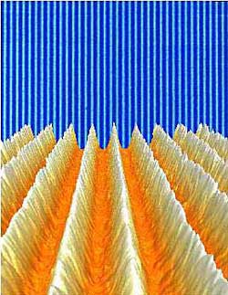
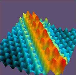
Laser-Focused Atomic Deposition. In this new form of nanofabrication, a laser standing wave propagates across a Si surface, concentrating atoms into its nodes as they deposit. Shown is a composite of two atomic force microscope images. The foreground is a three-dimensional rendering of an atomic force microscope image, showing 65 nm wide Cr lines. The background is a larger-range AFM image of the same sample, illustrating the regularity of the lines, which are spaced at exactly half the laser wavelength.

Reference: J.J. McClelland, R.E. Scholten, E.C. Palm, R.J. Celotta, Science 262, 877 (1993).

Laser-Focused Atomic Deposition

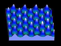
Laser-Focused Atomic Deposition of Nanodots. In this new form of nanofabrication, a laser standing wave propagates across a Si surface, concentrating atoms into its nodes as they deposit. Here, a two-dimensional standing wave creates an array of dots on the surface, spaced at exactly half the laser wavelength. The image is taken with an atomic force microscope on an array of Cr features on a Si surface. For this sample, the dots are spaced at 212.78 nm, and have height and width of 13 and 80 nm, respectively.

Reference: R. Gupta, J. J. McClelland, R. E. Scholten, Z. J. Jabbour, and R. J. Celotta, Appl. Phys. Lett. 67, 1378 (1995).

Laser-Focused Atomic Deposition of Nanodots.

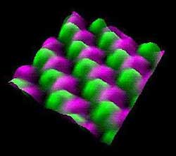
Colored Atoms in Compound Semiconductor Surfaces. Two superimposed STM imagesof the gallium arsenide (110) surface obtained at two different tunneling voltages. The green image shows the position of the gallium atoms obtained when electrons tunnel into the surface and sample the predominately empty gallium surface states. The red image shows the position of the arsenic atoms obtained when electrons tunnel from the surface into the tip and sample predominately filled arsenic surface states. The combined image reconstructs the whole surface of the gallium arsenide (110) surface

Reference: L. J. Whitman, J. A. Stroscio, R. A. Dragoset, and R. J. Celotta, unpublished

Colored Atoms in Compound Semiconductor Surfaces.

Self-Assembly of Atomic Wires. STM image showing zig-zag chain of cesium atoms (red) on a gallium arsenide (110) surface (blue). The image size is 7x7 nm. These atomic wires form naturally by self-assembly when cesium atoms are deposited on the GaAs surface. The self-assemble process results from cesium atoms diffusing on the surface and searching out the ends of existing cesium chains, which are preferential sticking sites.

Reference: L. J. Whitman, J. A. Stroscio, R. A. Dragoset, and R. J. Celotta, Phys. Rev. Lett. 66, 1338 (1991).

Self-Assembly of Atomic Wires.

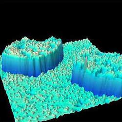
Atomic Scale Alloying. STM image, 35nm x 35nm, showing atomic scale alloying of chromium atoms (small yellow bumps) on an iron (001) surface when chromium atoms are deposited on the iron surface. The two islands are single atomic steps composed of iron atoms that were kicked out of the surface by the deposited chromium atoms. The islands also show alloyed chromium atoms. The chromium atoms reside in an iron lattice site and are a substitutional impurity. The chromium impurities at the iron-chromium interface have a significant effect on magnetic properties of films composed of layers of iron and chromium layers.

Reference: A. Davies, J. A. Stroscio, D. T. Pierce, and R. J. Celotta, Phys. Rev. Lett. 76, 4175 (1996).

Atomic Scale Alloying.

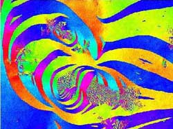
Domain Structure Near a Defect in an Amorphous Ferromagnet. The magnetic domain structure of an amorphous magnetic ribbon revealed by the technique of scanning electron microscopy with polarization analysis. The colors in this image correspond to different magnetization directions. This type of ribbon is commonly used in the magnetic core of power line transformers. Defects, such as the one in the center of this image, interact with the magnetic domain structure, interfering with the domain wall motion. These interactions result in energy losses that reduce transformer efficiencies.

Work done in collaboration with Allied Signal Corp. John Unguris, Electron Physics Group, NIST

height:250px; padding:5px;

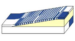
Magnetic Coupling in Fe/Cr/Fe. This figure shows the magnetic coupling between an Fe film and an Fe crystal separated by a wedge-shaped Cr spacer layer. The indirect coupling through the spacer switches from ferromagnetic (aligned Fe magnetizations) to antiferromagnetic (opposed magnetizations) with every single atom thick change in Cr layer thickness. The magnetic domain structure of the Fe film is imaged using scanning electron microscopy with polarization analysis, and it is shown superimposed on a schematic of the wedge structure. Black and white contrasts in the image correspond to opposite magnetization directions.

Reference: "Observation of Two Different Oscillation Periods in the Exchange Coupling of Fe/Cr/Fe(100)", J. Unguris, R.J. Celotta, and D.T. Pierce, Phys. Rev. Lett.. 67, 140 (1991)

Magnetic Coupling in Fe/Cr/Fe.

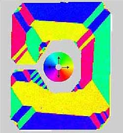
Patterned Magnetic Element. Scanning Electron Microscopy with Polarization (SEMPA) image of the magnetic domain structure of a patterned Fe thin film structure. This C-shaped structure, produced at the Naval Research Labs, is a prototype magnetic device for use in hybrid magnetoelectronic circuits. The element is 100 mm tall and about 50 nm thick. The direction of the magnetization is coded into color as given by the color wheel in the center of the image.

Reference: John Unguris, Electron Physics Group, NIST

Patterned Magnetic Element.

Wide-band Gap Semiconductors

Blue light emitting diode containing a GaN/InGaN double heterojunction and fabricated with a stripe geometry.

Wide-band Gap Semiconductors